EUV is the acute ultraviolet lithography machine made by one firm in the entire world, Dutch agency ASML. The machine etches circuitry patterns onto silicon wafers utilizing extraordinarily skinny traces to assist with the location of elements positioned inside a chip. A number of layers are required for the processors utilized in smartphones.
Samsung Foundry will use roughly 26 EUV layers for its 2nm manufacturing subsequent yr
Samsung Foundry presently makes use of 20 EUV layers with its present 3nm manufacturing and a 30% improve would lead to 26 layers for its 2nm chips. Extra EUV layers ought to lead to extra transistors discovered inside a chip making the SoC in a position to deal with extra complicated duties whereas consuming much less battery energy. Samsung’s 2nm chipsetsd can be 17% smaller than the current-generation chipsets, 18% extra highly effective, and 15% extra environment friendly.
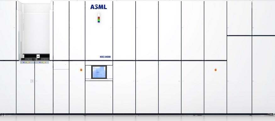
ASML expects to ship 60 of those first-generation EUV lithography machines this yr. | Picture credit-ASML
In addition to utilizing an elevated variety of EUV layers, at 2nm Samsung Foundry will use bottom energy supply community (BSPDN). This tech is chargeable for the 17% decline in chipset dimension by shifting the facility provide traces to the bottom of a chip as an alternative of the entrance. This reduces voltage drop as a result of the traces might be made larger due to having extra room. This expertise, additionally utilized by Intel with its PowerVia characteristic, makes chipsets extra highly effective and environment friendly.
Looking forward to 2027 when Samsung Foundry is anticipated to start manufacturing utilizing its 1.4nm node, the variety of EUV layers is anticipated to rise to greater than 30. And as soon as once more the transistor rely will rise and utility processors can be extra highly effective and energy-efficient than they’re at present. Samsung Foundry’s chief rival is trade chief TSMC and the Taiwan-based foundry makes use of as much as 25 EUV layers for its present 3nm (N3x) manufacturing.
Samsung Foundry began using EUV lithography in 2018 when it moved from 10nm to 7nm. Earlier than EUV lithography, the trade used DUV (or deep ultraviolet) lithography. Samsung Foundry can be utilizing EUV for DRAM manufacturing with seven layers used within the manufacturing of its Gen 6 10nm DRAM chip. SK Hynix, one other DRAM designer and producer, makes use of 5 EUV layers.
Just one firm makes and sells EUV machines
ASML is anticipating to ship much more EUV lithography machines this yr. Every one is the dimensions of a faculty bus and prices as much as $183 million for the previous-generation mannequin and as much as $380 million for the Excessive-NA second-gen machine. TSMC will reportedly obtain 70 first-generation EUV machines from ASML in 2024 and 2025 as a result of sturdy demand for chips produced utilizing its 3nm and 2nm nodes. Like Samsung Foundry, TSMC will begin producing 2nm chips subsequent yr with its 1.4nm node anticipated to be employed in 2027-2028.
Whereas the previous-generation EUV machines have an aperture of .33, the Excessive NA machines have an aperture of .55. Utilizing the Excessive-NA machine, a better decision sample is transferred to a wafer so {that a} foundry would not need to run a wafer via the EUV machine twice so as to add extra options. This protects each money and time. Samsung Foundry has reportedly bought at the least one Excessive-NA lithography machine however TSMC refuses to buy one of many new technology EUV machines for now.
👇Observe extra 👇
👉 bdphone.com
👉 ultraactivation.com
👉 trainingreferral.com
👉 shaplafood.com
👉 bangladeshi.help
👉 www.forexdhaka.com
👉 uncommunication.com
👉 ultra-sim.com
👉 forexdhaka.com
👉 ultrafxfund.com
👉 ultractivation.com
👉 bdphoneonline.com
👉 Subscribe us on Youtube